Gunn diode is a two-terminal but a bulk device, without any junction. It is also called a diode as it has two terminals. Gunn diodes are also −ve resistance device, normally used as low-power oscillators at microwave frequencies in transmitters, local oscillators of receiver front end.
Table of Contents
Gunn Diode
In 1963, J. B. Gunn observed a periodic variation of current passing through an N-type GaAs semiconductor. He found the following when a DC bias voltage is applied to the contacts of N-type GaAs or InP:
- The current first rises linearly from zero.
- Then, it begins to oscillate when a certain threshold is reached.
- The time period of oscillation is equal to the travel time of electrons from the cathode to anode.
This is known as Gunn effect or bulk effect. The device that shows the Gunn effect is known as Gunn diode. Gunn diodes are usually fabricated using N-type semiconductor materials (eg. GaAs, and InP); so, they should be associated with electrons rather than with holes.
Gunn diode operations do not depend on junction properties. Even though it has no junction, it is called a diode, because it has two terminals (anode and cathode) attached to it. It is an active two-terminal solid-state device and is mainly used as a local oscillator in the microwave frequency range of 1 to 100 GHz. Gunn effect can be explained on the basis of domain formation, two-valley theory of Ridley–Watkins–Hilsum (RWH), or the transfer electron mechanism.
Structure of Gunn Diode
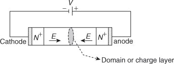
The Gunn diode is made up of a single piece of N-doped semiconductor material (e.g. GaAs, InP) with two thinner N+-doped layer contacts on opposite ends. The two N+ layers are required to connect the anode and cathode leads. The three-layer structure of Gunn diode is shown below.

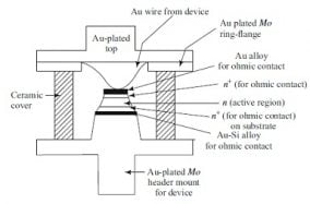
Gunn Diode Package and symbol
the device structure as well as the packaged diode, and n+ GaAs substrate, epitaxial layer of n-active layer is grown and then n+ layer diffused on it for ohmic contact.


Characteristics Curve
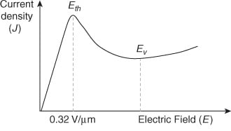
When a DC voltage (V) is applied to the two terminals, an electric field (Eo) will be established across the piece of GaAs (just as in a resistor). The curve between current density through the material and the electric field (Eo) is shown below.

We know that the drift velocity (vd), current density, and electric field have the following relations:
v_{d}=\mu \vec{E}
\vec{J}=nq\mu \vec{E}
Operation
Initially, when the electric field is increased, from the above relations it can be seen that the drift velocity and current density increase. Thus, the current density increases with an increase in the electric field, resulting in a positive resistance. This continues till the electric field reaches a value known as threshold value Eth (corresponding threshold voltage Vth).
When the electric field is increased beyond the threshold value Eth, the Gunn effect takes place and the current density decreases, causing the device to exhibit negative resistance. This behavior is due to domain formation, which will be explained in the next section. This will continue till the field reaches a value known as Ev (corresponding valley voltage). When the voltage is increased beyond Ev, the current density increases. Thus, the device again exhibits positive resistance.
Negative resistance region: In common the current first rises linearly from zero with increasing electric field, however there is a region between the threshold electric field and valley electric field, where the current decreases as the electric field is increased. This is called the negative resistance region. The dynamic resistance, r, in this voltage range is given by
r=dV/dI,r< 0
Domain Formation
When bias voltage (V) is applied across the diode terminals, an electric field (E0) is established across the GaAs piece. As E0 increases, electron drift velocity increases up to a certain potential (Eth). This is because the velocity (vd) is proportional to the applied electric field.
However, with a further increase in voltage, the mobility decreases, which causes the velocity to decrease, thereby causing the electrons to slow down. This slowing down results in a traffic jam, and more electrons pile up to form a charge layer or domain. This charge layer produces an electric field (E) such that it decreases the original field (E0) on the left and increases the original field (E0) to the right. As a result, the charge bunch gets pushed toward the anode on the right, forming a current pulse.

When this pulse moves to the anode, E0 goes back to the original value, resulting in another traffic jam and another pulse formation, which causes oscillation.
In this procedure, N-type GaAs releases the power that it has acquired during the domain formation in the direction of the anode. If conditions are appropriate, this release of power at anode will be utilized by the noise energy of suitable frequency existing in the Gunn diode configuration and gets amplified. The amplification of noise energy results in sustained oscillations. The frequency of oscillation depends on the length of the GaAs piece and the concentration of electrons.
RWH Theory or Two-valley Theory of Gunn Diode
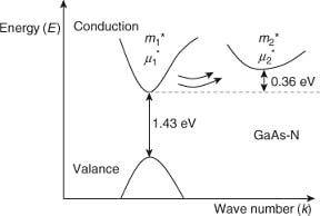
The Gunn diode, which is made of n-doped semiconductor material (e.g. GaAs or InP), is characterized by having two valleys in their conduction bands with different mobility. The two-valley model is also called the Ridley–Watkins–Hilsum (RWH) theory. There are two regions in the conduction band of the N-type GaAs. These conduction band regions are known as an upper valley and lower valley. The energy band and transfer of electrons between the two valleys are shown in figure below.
Key points of GaAs
- In N-type GaAs, the valence band is filled with electrons, and the conduction band is partly filled.
- The forbidden energy gap between the valence band and the conduction band is about 1.43 eV.
- Electrons in the lower valley (n1) exhibit a small effective mass (m1) and very high mobility, μ1.
- Electrons in the upper valley (n2) exhibit a large effective mass (m2) and very low mobility, μ2.
- The two valleys are separated by a small energy gap, ΔE, of approximately 0.36 eV. At a low electric field, electrons remain in the lower valley and material behaves ohmically. When the electric field reaches a certain threshold value Eth, the electrons will be swept from the lower valley to the upper valley. If the rate of transfer of electrons from the lower to the upper valley is very high, the current will decrease with an increase in voltage.
- The average electron mobility, μ is given by
\mu =(n_{1}\mu _{1}+n_{2}\mu _{2})/(n_{1}+n_{2})
where
- n1 = electron density in lower valley
- n2 = electron density in upper valley
- μ1 = mobility of electron in lower valley
- μ2 = mobility of electron in upper valley
- Total carrier concentration = n1 + n2

where m1* = effective mass of electron in lower valley
m2* = effective mass of electron in upper valley
Typical Characteristics
The voltage of operation depends on the active layer width. As the device has to operate between Eth (3.3 kV/cm) and Emin (11 kV/cm) say at E0 = 6 kV/cm. The current density at 6 kV/cm is 400 A/cm2.
Therefore requirement of bias depends on active layer width, e.g. for L = 5 µm, V = 3 V and for L = 50 µm, V = 30 V. Therefore for 3×10⁻⁸ m2 area, I = 120 mA. With the above, the characteristic of a typical diode may be as:
- CW power = 25 mW to 250 mW X band (5 – 15 GHz)
- 100 mW at 18-26.5 GHz
- 40 mW at 26.5-40 GHz
- Pulsed Power = 5W (5-12 GHz)
- Efficiency = 2–12%
- Frequency Tuning: The frequency of Gunn oscillator can be changed by mechanical tuning and electronic tuning.
Applications of Gunn Diode
- It is used in Radar transmitters as a low power oscillator (e.g. CW Doppler Radar, Police Radar).
- Gunn diode oscillators with pulse signals are used in transponders in industry telemetry systems and for air traffic control.
- It is used in a broadband linear amplifier.
- Gunn diode is used in sequential logic circuits and fast combinational circuits.
- It is used in microwave receivers as low and medium power oscillator.
- It is used in a parametric amplifier as pump sources.


