Try Visual Search
Search with a picture instead of text
The photos you provided may be used to improve Bing image processing services.
Privacy Policy
|
Terms of Use
Drag one or more images here or
browse
Drop images here
OR
Paste image or URL
Take photo
Click a sample image to try it
Learn more
To use Visual Search, enable the camera in this browser
All
Images
Inspiration
Create
Collections
Videos
Maps
News
Shopping
More
Flights
Travel
Hotels
Search
Notebook
SafeSearch:
Moderate
Strict
Moderate (default)
Off
Filter
Autoplay all GIFs
Change autoplay and other image settings here
Autoplay all GIFs
Flip the switch to turn them on
Autoplay GIFs
Image size
All
Small
Medium
Large
Extra large
At least... *
Customized Width
x
Customized Height
px
Please enter a number for Width and Height
Color
All
Color only
Black & white
Type
All
Photograph
Clipart
Line drawing
Animated GIF
Transparent
Layout
All
Square
Wide
Tall
People
All
Just faces
Head & shoulders
Date
All
Past 24 hours
Past week
Past month
Past year
License
All
All Creative Commons
Public domain
Free to share and use
Free to share and use commercially
Free to modify, share, and use
Free to modify, share, and use commercially
Learn more
Clear filters
2000×1333
waferworld.com
Common Causes of Damage or Failures Found in Silicon Wafer Substrates
372×372
ResearchGate
Example of precise silicon wafer shaping by thin lay…
551×511
ganwafer.com
Thin Film Deposition and Metallization on Silicon Waf…
850×479
mungfali.com
Silicon Wafer Process
850×665
ResearchGate
Silicon Wafer Processing. A) Silicon Wafer Substrate Preparation. 1 ...
1000×750
waferworld.com
who offers a silicon wafer processing?
2000×1285
waferworld.com
Silicon Wafer Processing | What You Need to Know About Metallization
509×339
iStock
Loading A Silicon Wafer Into A Deposition Coating Machine Used In …
600×600
microdispersion.com
Silicon Wafer Undoped - NanoChemazone | Se…
1622×524
chegg.com
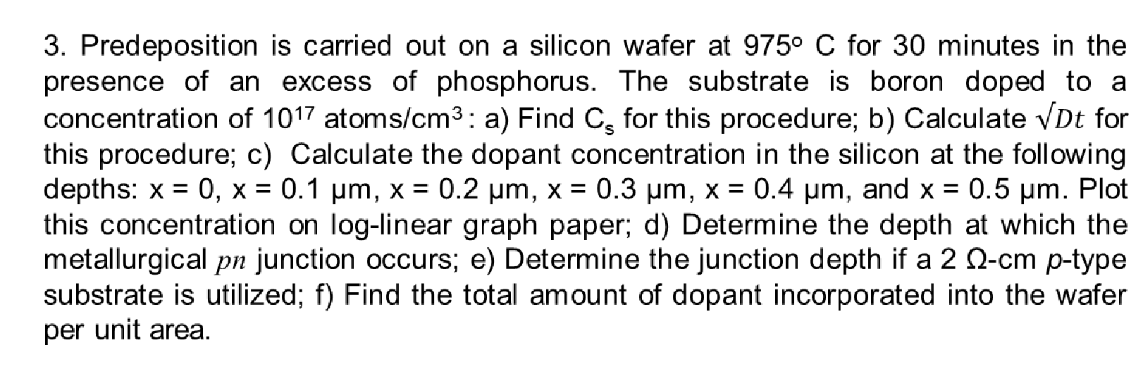
Solved 3. Predeposition is carried out on a silicon wafer at | Chegg.com
924×693
chegg.com
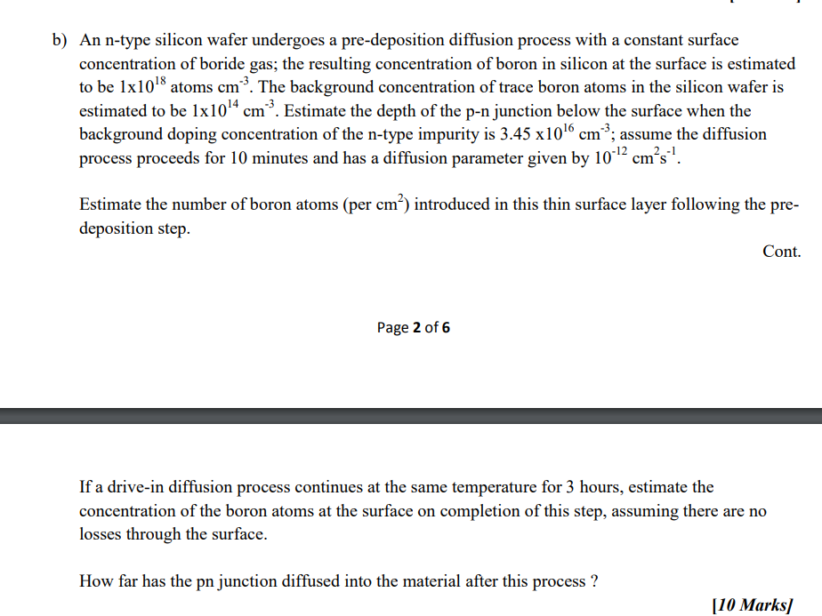
Solved b) An n-type silicon wafer undergoes a pre-deposition | Che…
1024×768
slideserve.com
PPT - The applications and uses of LPCVD silicon nitride deposition ...
850×893
ResearchGate
115 questions with answers in SILICON WAFER | Science topic
768×576
studylib.net
Silicon Deposition
664×208
ResearchGate
Process steps: (1) bare silicon wafer, (2) Ti-Cu deposition, (3 ...
768×918
ResearchGate
97 questions with answers in SILICON W…
450×337
Cambridge University Press
Liquid metal deposition process developed for wafer-scale 2D semiconductors
642×415
cambridge.org
Liquid metal deposition process developed for wafer-scale 2D semiconductors
725×492
ResearchGate
Silicon dioxide and aluminum deposition on a wafer to validate the FEM ...
640×640
ResearchGate
Silicon dioxide and aluminum deposition on a wafer to valid…
640×640
researchgate.net
Backside of a silicon wafer after the first deposition (l…
850×490
researchgate.net
Backside of a silicon wafer after the first deposition (left) and the ...
640×640
researchgate.net
Pictures of the Silicon wafer after each step of …
1024×768
insidetheiot.com
Removing Materials from a Silicon Wafer - Inside the IoT
693×263
researchgate.net
Actual view of the silicon wafer after processing. | Download ...
263×263
researchgate.net
Actual view of the silicon wafer after processing…
500×370
pinterest.com
SEM images of the silicon wafer with silver dendrites grown at 50 …
850×511
researchgate.net
Deposition on silicon wafers. A) Thickness of PDA coatings deposited on ...
1000×653
alamy.com
Silicon wafer closeup Stock Videos & Footage - HD and 4K Video Clips ...
655×333
acldigital.com
Silicon Wafer Manufacturing in the Semiconductor Industry | ACL Digital
850×575
researchgate.net
The sample drilled out from the silicon wafer showing, (a) a photograph ...
850×206
researchgate.net
The initial phase of transforming a silicon wafer into a ribbed and ...
850×427
researchgate.net
25: SEM images of the material transferred to a silicon wafer surface ...
474×472
platypustech.com
Why Coat Silicon Wafers with Metal Surfaces?
640×640
researchgate.net
28: Bonded wafers after removal of the silicon h…
Some results have been hidden because they may be inaccessible to you.
Show inaccessible results
Report an inappropriate content
Please select one of the options below.
Not Relevant
Offensive
Adult
Child Sexual Abuse
Feedback
 Feedback