By Terence Graham and Bonnie Mack,
Ciena Corporation
Introduction
In Part 1 of this article [1] the overall thermal environment for pluggable optical modules (POMs) was described, with the effect of both out of flatness and source locations relative to heatsink contact area also examined. The article also introduced the relevant sections of the multi-source agreements (MSAs) [2-5] and optical internetworking forum (OIF) thermal interface specifications [6]. In this article (Part 2), the results are extended to examine the effects of heat sources on the carrier printed circuit board (PCB) and their relation to the calibration of internal temperature sensors of a C-form-factor-pluggable 2 (CFP2) transceiver model with a generic zinc-alloy-case. This was done by exploring the heat exchange between it and both the carrier PCB and heatsink.
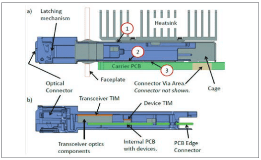
This article delves further into the influence of the thermal interface location and its size relative to the internal PCB heat source location on the cooling of another form factor, Quad Small Form-factor Pluggable (QSFP). The QSFP is a common POM that presently has the highest power density of all the form factors [7]. The complete QSFP and cage assembly is shown in Figure 1 and described further in [1,8]. CFP2 POM and cage are similar but larger.

The numerical analysis presented in this article was undertaken using commercially available computation fluid dynamics (CFD) software, with complete modelling details provided in [8]. Key modeling aspects are discussed here. Air thermophysical properties were modelled at 50 °C and 1800 m elevation conditions. These are operating temperature limits for telecommunication equipment from GR-63-Core [9]. For the CFP2 and QSFP modules the upstream air flow velocity was set at 2 m/s and 1.5 m/s, respectively. These cooling air flow speeds lie within the typical range for POM environments. Other analysis variables are summarized in the appropriate section.
No experimental results are presently available for the configurations studied here, but measurements on commercial product PCBs with thermal mock-up POMs that used the same modelling techniques and software have shown good design level accuracy to predicted temperatures, and to trends in internal sensor calibration as a result of PCB heating. On this basis, confidence is established on the accuracy of the numerical predictions presented in this article.
Calibration of Numerical Wind Tunnel Geometry for CFP2 Heat-Flow Analysis
The wind tunnel geometry, location of the carrier PCB heat sources, and temperature sensors are shown in Figure 2. Three carrier PCB heating layouts are used to simulate local processors or other power dissipating components and are summarized in Table 1. The geometry of the CFP2 modeled in [1] was updated with more detail for the heat sources and their connection to its lid and base. The internal power dissipation of CFP2 was reduced from 12 W to 9 W, so as put its operation into power density class 4 (pd04) [7]. In this case the thermal interface contact area is modelled as perfectly flat (0 mm) with 0.119 °C/W thermal resistance representing 15 N contact force and 1.6 µm Ra finish per the MSA specification [2]. The test case variables for CFP2 heat-flow analysis are summarized in Table 1.

Thermal insulation was added to the carrier PCB, Figure 2, to evaluate its effectiveness in controlling heat flow when calibrating the internal front and rear temperature sensors. The CFP2 was also modelled with a cold plate (isothermal heatsink) in a natural convection environment. This was recommended in [7] for measuring the thermal interface contact resistance and for use in calibrating internal temperature sensors. In the insulation studies, 1 mm of insulation having a thermal resistance equivalent to approximately 2 mm of quiescent air, or 10 mm of dry wood, was applied to both sides of the carrier PCB to enforce heat removal via the heatsink, or cold-plate, rather than directly to the air.

POMs usually have internal sensors that can monitor the module operating temperatures and are calibrated across the product specified operating temperature range. The front and rear sensor locations in the POM, Figure 2, are representative locations for such sensors. The CFP2 model has two sensors on the secondary side of the internal PCB. One is centered under the two front heat sources. The other is centered just behind the two rear heat sources. Details of the internal design parameters of the CFP2 are en in [8].

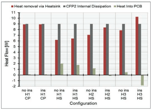
Figure 3 shows the predicted heat flows from the CFP2 module to both its heatsink and the carrier PCB for several insulation and PCB heat dissipation conditions. It shows that for carrier PCB heating layouts H1, a cold plate and natural convection environment, over 99% of the CFP2 dissipation is removed across the thermal interface area. In contrast, with a heatsink instead of a cold plate attached, less than 72% of the heat is removed through the heatsink, even with an insulated carrier PCB. The results for carrier PCB heating layouts H2 and H3 show significant conduction from the carrier PCB into the POM when the PCB is insulated.
The nominal thermal resistance for the CFP2-heatsink interface area, rInt, is defined as in [7]:
rInt = ΔT MP-HS / (PCFP2 / AInt ) [m2°C /W]
where:
TMP = Temperature at CFP2 lid “Hot Spot” monitor point [°C],
AInt = Thermal interface area [m2], PCFP2 = CFP2 power dissipation [W],
ΔT MP-HS = Temperature difference between the CFP2 lid “Hot Spot” (TMP) and center of heatsink contact pad [°C]
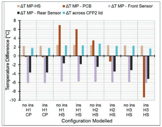
As defined, rInt includes the effects of heat spreading in both the CFP2 lid and heatsink base. Figure 4 compares TMP to temperatures differences with the front and rear sensor locations. In the current model, the difference between TMP and the front-sensor-temperature, ΔTMP-Front Sensor, remain relatively constant, i.e. less than 0.4°C, over the thermal environments modelled while ΔTMP-rear sensor varies by more than 4.5°C. Consequently the front temperature sensor would be the better choice to calibrate to represent the monitor point since its dependence on heat conducted from the carrier PCB is minimal. The variation in the rear sensor temperature is more than the typical accuracy specification of ±3°C. Therefore, the cold plate method would be the most repeatable for calibration.

Using a cold plate, the predicted thermal resistance should be reasonably accurate since over the majority of the heat flows through the heat sink thermal interface area (AInt), and cold plate base, will be uniform by design. With a cold plate, rInt is twice the nominal applied contact resistance of 3.2 °C-cm2/W. Spreading effects in the CFP2 lid accounts for this added resistance even with good distribution of the heat sources. ΔT MP-HS remains greater than the 2°C specification [7] for high performance interfaces. Even assuming perfect flatness, the MSA maximum of 1.6 µm Ra surface finish is clearly not sufficient for the 9W dissipation of this CFP2 POM for a high temperature ambient.
QSFP Model – Expanding on the Effect of Spreading Resistance
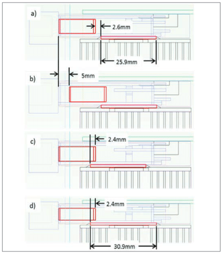
The majority of QSFP heat is dissipated close to the faceplate and not directly underneath the heatsink contact area. A numerical wind tunnel study was conducted to explore the internal thermal resistances and develop methods of reducing the QSFP temperatures. The numerical model shown in Figure 5 is detailed in [8] and is similar to that of [10] having a 5 W QSFP and a power density of 1.34 W/cm2, class pd14 [7]. Cooling was via a typical aluminum off-the-shelf heatsink. The model was used to predict the effect of changes in the heat source locations relative to the nominal heatsink contact area, i.e. the thermal interface area of reference [7], is shown Figure 5. For scenario (d) the 5 mm extension of the heatsink contact area towards the transceivers, the power density decreases to 1.14 W/cm2 or to class pd12 [7].

As with the CFP2, contact resistance with the heatsink was estimated per the method of [11] for a perfect flatness at two different surface roughness and load conditions: Rc1 for 1.6 µm Ra and 5 N contact force, and Rc2 for 0.6 µm Ra finish and 10 N contact force. Results were calculated for QSFP case material thermal conductivities of 116, 169, 385 and 1000 W/m-K corresponding to a zinc alloy, high grade aluminum casting, copper and an ultra-high conductivity material respectively.
The temperature difference results shown in Figure 6 illustrate the importance of the surface finish of the case (controlled by POM design) and heatsink (controlled by system design), and of locating the heat sources and the thermal interface area as closely together as possible. QSFP MSA cage dimensions [4, 5] allow an increase in heatsink contact length by up to 5 mm. In the current model this larger contact resulted in a temperature decrease of more than 1.5 °C with zinc alloy case and Rc1. If the case material conductivity is increased to 169 W/m-K or 385 W/m-K, further decreases of 1 C to 2 °C, respectively, could be achieved (solid orange line). While very high case conductivity representing an exotic material was examined, changing QSFP case material to copper from zinc alloy can improve performance by 1.5°C to 3 °C for MSA heatsink contact design (solid red line).
Decreasing the contact resistance to Rc2 would bring total improvement to approximately 5 °C (solid red zinc alloy to dashed red copper). These are significant when the overall ambient to case temperature budget could be 15 °C or less for downstream components in a Telcordia environment [12].
Even with these potential gains the high power density of the QSFP means it is unlikely that the OIF high performance interface specification of 2 °C between the monitor point and the heatsink will be attained for plug dissipation greater than 4.2 W.

Discussion
The OIF agreement [7] specifies information required by system designers for preliminary, simplified system, and detailed system analyses. Simple estimations of the temperature loss to the heatsink are feasible by defining power density classes and requiring a measurement of the overall thermal resistance between the monitoring point on the POM module lid and the heatsink. This measurement is to be done on a module in its cage, and powered from an insulated carrier PCB with a cold plate heatsink to ensure the thermal interface resistance measurement includes the POM’s contribution to the interface resistance. For this environment, the results presented here show that 99% of the CFP2 dissipation flows through the interface of interest, whereas other test methods have net heat transfer from the POM to the carrier PCB, or to the POM from the carrier PCB.
Final POM module thermal assessment is at present only available with a computationally expensive detailed model created from the information specified in [7] and either built by the system designer with information from the module supplier, or is a model supplied by the module vendor, likely under some form of non-disclosure agreement (NDA). An alternative to this approach has not yet been explored is the development of a Delphi-type resistance network [13]. A model of this type could be used to model the connections to the carrier PCB, surrounding air and heatsink with distributed internal heat sources similar to a multi-junction integrated circuit device. This could be provided by POM module vendors without giving internal details of the module.
Summary
Thermal interface resistance of pluggable optical modules (POMs) is affected by design factors under the control of both the system and module designers. In particular, surface finish and flatness have a strong influence within normally accepted manufacturing and machining practices.
POM designers can reduce thermal spreading losses by keeping the heat sources close to the thermal interface area and by increasing the thermal conductivity of the case materials. For Quad Small Form-factor Pluggables (QSFPs), the size of the cage hole for heatsink contact given in the multi-source agreement (MSA) can be increased giving a reduction in the thermal interface resistance and therefore module temperature.
The Optical Internetworking Forum (OIF) definition of thermal interface gives a useful division of the responsibilities for module cooling at the module case. The thermal interface resistance is defined for an ideal heatsink contact on the system side so that POM designers can optimize module surface contact and spreading thermal resistance.
Figures 3 and 4 highlighted the importance of the heat paths between the POM and the carrier printed circuit board (PCB). In the absence of junction-to-board thermal resistance (Rj-b) type information, thermal assessments are biased towards lid-only cooling. Real applications include the effects of the carrier PCB. Optical module designers should therefore consider a thermal resistance network model of their optical plugs to complement the thermal interface information defined in the OIF Implementation Agreement (IA).

received his B.Sc. degree in Mathematics and Engineering from Queen’s University, and his M.A.Sc. and Ph.D. in Aerospace Studies from University of Toronto. He has 15 years of experience in electronics cooling system design and development for optical networks and concentrating solar photovoltaic systems. He is currently a senior thermal engineer at Ciena who isactive in the Optical Internetworking Forum. Previously he worked with Nortel, Atomic Energy of Canada, and University of Toronto. He has more than 20 articles in archival journals and conference proceedings in the areas of air cushion technology, sealing technology, ice slurry equipment, and in thermal design and development for optical telecommunications systems.

has been working in electronics cooling for over 25 years. She has worked at Nortel, Solectron and as an independent contractor. She is currently a senior thermal engineer at Ciena specializing in thermal simulation and testing. She is a past chair of the Semi-Therm conference and currently serves on the program committee. She is a past member of the Harvey Rosten Award for Excellence selection committee. She received a B.A.Sc. and a M.A.Sc. in engineering at the University of Waterloo.
Contact Information
Terence Graham, Bonnie Mack
Ciena Corporation
3500 Carling Ave.
Ottawa, Ontario, Canada
Email: [email protected]; [email protected]
References
[1] Mack, B., and Graham, T., “Pluggable Optics Module – Thermal Specifications, Part 1,” Electronics Cooling, June 2016, https://electronics-cooling.com/2016/07/pluggable-optics-modules-thermal-specifications-part-1/, accessed August 13, 2016.
[2] Hiramoto, K., “CFP MSA CFP2 Hardware Specification,” Revision 1.0, July 2013, http://www.cfp-msa.org/Documents/CFP2_HW-Spec-rev1.0.pdf, accessed August 13, 2016.
[3] Oomori, H. Hardware Technical Editor, CFP MSA CFP4 Hardware Specification, Revision 1.0, August, 2014, http://www.cfp-msa.org/Documents/CFP-MSA_CFP4_HW-Spec-rev1.0.pdf, accessed August 13, 2016.
[4] SFF Committee, “SFF-8663 Specification for QSFP+ 28 Gb/s Cage (Style A),” Revision 1.5, April 2014, ftp://ftp.seagate.com/sff, , accessed August 13, 2016.
[5] SFF Committee, “SFF-8661 Specification for QSFP+ 28 Gb/s 4x Pluggable Module,” Revision 2.0, February 2014, ftp://ftp.seagate.com/sff, accessed August 13, 2016.
[6] Optical Internetworking Forum, www.oiforum.com, accessed August 13, 2016.
[7] IA# OIF-Thermal-01.0, “Implementation Agreement for Thermal Interface Specification for Pluggable Optics Modules,” Optical Internetworking Forum, May 2015, http://www.oiforum.com/wp-content/uploads/OIF-Thermal-01.0_IA.pdf, accessed August 13, 2016.
[8] Mack, B., Graham, T., “Thermal Specifications for Pluggable Optics Modules,” in 32nd Thermal Measurement, Modeling & Management Symposium (SEMI-THERM), San Jose, CA, USA, March 14-17, 2016, pp. 133-142.
[9] Telcordia, NEBS Requirements: Physical Protection, Telcordia Technologies Generic Requirements, GR-63-CORE, Issue 3, March 2006.
[10] OIF-PLUG-Thermal-01.0, “Thermal Management at the Faceplate White Paper,” Optical Internetworking Forum, March 2012.
[11] Yovanovitch, M.M., Culham, J.R., and Teerstra, P., “Calculating Interface Resistance,” ElectronicsCooling, May 1997, https://electronics-cooling.com/1997/05/calculating-interface-resistance/, accessed August 13, 2016.
[12] TelcordiaTechnologies Generic Requirements, Generic Requirements for Telecommunications Data Center Equipment and Spaces, GR-3160-CORE, Issue 2, July 2013, http://telecom-info.telcordia.com/ido/AUX/GR_3160_TOC.i02.pdf, accessed August 13, 2016.
[13] Lasance, C.J.M “Ten Years of Boundary-Condition Independent Compact Thermal Modeling of Electronic Parts: A Review,” Heat Transfer Engineering, Vol. 29, Issue 2, pp. 149 – 168 (2008).


