Bipolar Junction Transistor (BJT) - Basic Structure and Operation
Published
A transistor is an electronic device that can be used as an amplifier or as an electronic switch. Its ability to amplify a signal or to switch high power loads using a small signal makes it very useful in the field of electronics. There are two basic types of transistors, the bipolar junction transistor, or BJT, and the field-effect transistor, or FET. In this tutorial, we will just focus on the bipolar junction transistor and discuss its basic structure and operation.
The term bipolar refers to the use of both holes and electrons as current carriers in the transistor structure.
Bipolar Junction Transistor (BJT) Structure
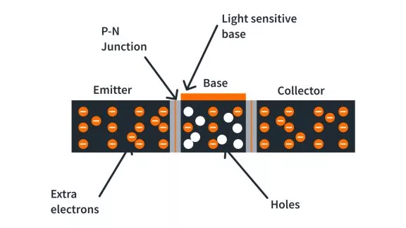
The bipolar junction transistor (BJT) is manufactured with three semiconductor regions that are doped differently. If we’ve already lost you with that last sentence, please go check out some of our other tutorials on the basics of semiconductors, as it’ll make this a lot easier to understand. These three regions that are doped differently are known as the base, collector, and emitter. The base region is lightly doped and is very thin compared to the collector and emitter regions. The collector region is moderately doped while the emitter region is heavily doped.

Bipolar junction transistors (BJT) can be an npn or a pnp type. The npn type consists of two n regions separated by a p region. The base region is the p-type material while the collector and emitter regions are n-type materials. In pnp type, the transistor consists of two p-type regions, the collector and emitter, separated by an n-type base region. Regardless of the type, a BJT has two pn junctions that must be correctly biased with an external DC voltage to operate properly. One of these junctions is called the base-emitter junction, connecting the base and emitter regions and the other one is the base-collector junction, connecting the base and collector regions.
Basic BJT Operation
In order for a bipolar junction transistor to operate as an amplifier, its base-emitter junction must be forward-biased while the base-collector junction is reverse-biased - please note that this means that an npn transistor and a pnp transistor are backwards compared to each other. And, as mentioned earlier, the emitter region is heavily doped. So in an npn transistor, the n-type emitter region has a very high density of free electrons while in a pnp transistor the p-type emitter region has a very high density of holes.

At this point, I’d like to remind you that current and electron flow are backwards, which may cause confusion. Since the base-emitter junction is forward-biased, free electrons from the emitter region easily cross the base-emitter junction and go into the very thin and lightly doped p-type base region. The p-type base region is just lightly doped, which means that, it doesn’t have that many holes in it. In this case, only a small percentage of the free electrons from the emitter region can recombine with the holes in the base region.
The small number of free electrons from the emitter region that recombined with the holes in the base region move through the base region as valence electrons. But when they leave the base region and move through the metallic base lead, they become free electrons and produce the external base current, which then goes out through the metallic lead, into the external circuit, and then, eventually, return to the emitter region.

The free electrons that entered the base region but didn’t recombine with the holes move toward the reverse-biased base-collector junction. Since the collector region is connected to the positive side of the external bias voltage, the free electrons are attracted to the positive side and are swept across into the collector region. They exit the collector region and and also move through the metallic collector lead, into the circuit, and return into the emitter region. So in this case, we know that the emitter current is the sum of the base and collector currents. Therefore, the emitter current is slightly greater than the collector current.
The operation inside a pnp transistor is very similar to the npn type. But the roles of the electrons and holes are swapped. The external bias voltages and the current directions are all reversed.

If you try to understand it, reversing the external bias voltages will forward bias the base-emitter junction of a PNP transistor and reverse bias the base-collector junction. Since the base-emitter junction is forward-biased, holes in the emitter region can move through the base-emitter junction and enter the base region. At the same time, electrons in the base region can also move into the emitter region. Inside the PNP transistor, the emitter current is due to the movement of holes from the emitter to the base region. But externally, emitter current is due to the movement of electrons from the emitter region to the positive terminal of the external bias voltage. The base current produced in a PNP transistor is due to the movement of electrons from the external bias voltage into the base region.
Since the base region is just lightly doped, only a small number of electrons in the base region recombine with the holes from the emitter region, and the rest of the holes move into the collector region. Internally, this movement of holes into the collector region produces the collector current but externally, the collector current is the flow of electrons from the external bias voltage into the collector region.

If we compare the direction of the currents of an npn and a pnp transistor using conventional current flow, we’ll see that the flow of currents in the pnp transistor is just opposite to the flow of currents in the npn transistor.

Summary
In this tutorial, we’ve discussed the basic structure and the basic operation of a bipolar junction transistor (BJT). We learned that a bipolar junction transistor is composed of three doped semiconductor regions, has two basic types - npn and pnp, and both types have two pn junctions. We also learned how to bias a bipolar junction transistor in order for it to operate as an amplifier and discussed what’s happening inside an npn transistor. If you have any questions, leave it in the comments below and if you’ve found this interesting or helpful, give it a like and subscribe to our channel!

Get the latest tools and tutorials, fresh from the toaster.


