Xilinx-FPGA DNA reading method
Update Time: 2020-04-10 10:51:34
Each FPGA of Xilinx has a unique ID, which is Device DNA. This ID is equivalent to our ID card. It has been written in the eFuse register of the chip when the FPGA chip is produced. It has unmodifiable attributes because of the use of It is the fuse technology. It is worth noting that in the 7 series and before, this ID is 57bit, but it is 96bit under Xilinx's Ultraslace architecture.
Our general use scenario for FPGA DNA is for user logic encryption. Generally speaking, the user can logically read this Device DNA through a specific interface, and after a series of encryption algorithms, compare it with a string of encrypted bytes stored in the external Flash in advance. The resulting byte string is also obtained after the DNA is encrypted. After fpga loads the program, it can read the byte from flash for comparison. If it is the same, let the FPGA start the corresponding logic. If it is different, it means that the FPGA does not have With the authorization of the user, the user can logically shut down the logic function of the FPGA or even damage the hardware through some means.
How to get FPGA Device DNA, I will explain the two methods from JTAG and call source language, and open the core code for your reference.
The first one is obtained through JTAG. This method can be implemented in ISE's Impact or vivado. The following describes how to use Vivado or Device DNA. This is actually very simple. First, the board is connected to the PC through JTAG. In Flow Navigator-> PROGRAM Under the AND DEBUG interface, click the corresponding FPGA chip, click Hardware Device Properties, search for dna in the search, you can find Device DNA under REGISTER, and there is a corresponding article on how to obtain DNA under Impact. I will not go into details here.
Second, user logic is obtained by calling the source language. As for what the source language is, here is a tip to share with you. Generally, when we use the source language, we often cannot remember a large number of source language definitions, so how to quickly search for what we want The source language you want, in Vivado, there is a function of Language Templates, which can be found in Flow Navigator, which contains basically all the source language and some grammatical usage provided by Xilinx. Taking DNA reading as an example, we search for DNA, You can find the source language of DNA. Because the blogger uses the VU9P film, the source language of DNA_PORTE2 is used. For the 7 series and before, the source language of DNA_PORT is used. Both source languages can be found in Language Templates found.
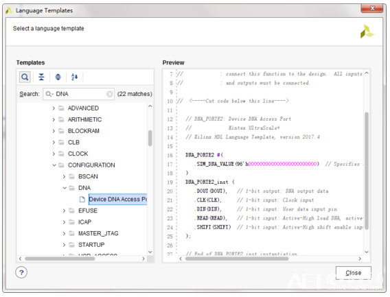
Next, let's talk about the use of this source language and the source language. This source language is essentially reading the FUSE_DNA register in the FUSE register table. It also contains a shift register. The interfaces in the source language are essentially operations. Shift register, the length of this shift register depends on the device type, it is 56 or 96bit. The READ signal in the source language is used to load the DNA value into the shift register, DIN is the input of the shift register, DOUT is the output of the shift register, SHIFT is the shift enable of the shift register, and CLK is The operation clock of the shift register, the source language model and timing diagram provided by the official are as follows

For users, to call this source language, we only need to operate according to the process of operating the shift register. Our purpose is to read the value of the shift register in the source language, so our design idea should be to pull up first READ first loads the shift register with the DNA value, and then enables SHIFT on the rising edge of the clock, so that the value in the shift register can be shifted out. The following is the core code:

This is a module of the axis bus. When dna_read_rdy is pulled high, the external is ready to receive data. At this time, the module reads the DNA value and sends it to the external module. When the external module receives the data and the dna_read_vld signal, it dna_read_rdy is pulled down A DNA value transmission process.
Previous: Everything about N-channel hexfet power mosfet-IRF3205
Next: Xilinx-7Series-FPGA high-speed transceiver use learning
Ratings and Reviews
Related Products
-
XC6SLX150-3CS484I
Xilinx
FPGA > -
XC4305PQ160C-5224
Xilinx
QFP > -

XCZU5CG-1SFVC784I
Xilinx
Zynq UltraScale+ MPSoC: CG Device SOC CO > -

XCZU4CG-2SFVC784I
Xilinx
Zynq UltraScale+ MPSoC: CG Device SOC CO > -

XC7Z030-1SBG485C
Xilinx
PSoC / MPSoC Microprocessor, Zynq-7000 P > -
XCKU035-2FBVA900I
Xilinx
Kintex UltraScale FPGA 468 I/O 900FCBGA > -

XC6VCX240T-2FFG1156I
Xilinx
Virtex-6 CXT FPGA 600 I/O 1156FCBGA > -

XCKU035-1SFVA784C
Xilinx
FPGA, Kintex UltraScale, 203128 Blocks, > -

XC7S15-1CSGA225I
Xilinx
Spartan-7 FPGA 100 I/O 225CSBGA > -

XC7A35T-1FGG484C
Xilinx
Artix-7 FPGAFPGA 250 I/O 484FBGA > -
XCV50E-6PQG240C
Xilinx
XCV50E-6PQG240C - NOT RECOMMENDED for NE > -

XCV405E-8BG560C
Xilinx
Extended Memory Field Programmable Gate > -
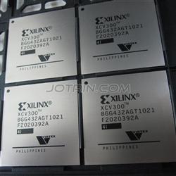
XCV300-4BGG432I
Xilinx
XCV300-4BGG432I - NOT RECOMMENDED for NE > -

XCV200-6BG352I
Xilinx
Field Programmable Gate Arrays > -
XCV150-4FG256C
Xilinx
Field Programmable Gate Arrays >
Hot Stocks
More- XCS40-3PQ208I
- XCS30-4TQG144C
- XCR5064-10VQ44I
- XCR3032XL-10CS48C
- XC9572XL-7VQG64C
- XC9572XL-7TQ100C
- XC9536XL-5VQG44C
- XC9536XL-10PC44C
- XC95288XL-7FGG256C
- XC95144-7PQ100C
- XC95108-10TQG100I
- XC7VX690T-3FFG1927E
- XC6SLX75-2FGG484I
- XC6SLX25T-3CSG324I
- XC6SLX16-3FT256I
- XC6SLX16-2CSG225I
- XC5VLX85-2FFG676I
- XC5VLX330-2FFG1760I
- XC5VLX220T-1FF1738C
- XC5VFX70T-2FFG1136I
- XC5VFX130T-1FFG1738I
- XC4VLX25-10FFG676I
- XC4VFX100-10FF1152C
- XC4036XLA-07HQ240C
- XC4013XL-3PQ160C
- XC4008E-2PQ160C
- XC4003H-6PQ208C
- XC4003E-3VQ100C
- XC3SD1800A-4CS484I
- XC3S50-5VQ100C
- XC3S5000-4FG900C
- XC3190A-3PQ160C
- XC3142A-5PC84C
- XC3142A-4PQ100C
- XC3130A-1PCG68C
- XC2VP30-5FFG1152I
- XC2V1000-4FGG456C
- XC2S50E-6TQG144C
- XC2S30-5CSG144I
- XC2S30-5CS144C
- XC2S15-6TQ144C
- XC2C256-7VQ100C
- XC2C128-7CPG132I
- XC17V16PC44C
- EF-DI-DISPLAYPORT-SITE


 ALL CATEGORIES
