Zen 3
2020 AMD 7-nanometer processor microarchitecture From Wikipedia, the free encyclopedia
Zen 3 is the name for a CPU microarchitecture by AMD, released on November 5, 2020.[2][3] It is the successor to Zen 2 and uses TSMC's 7 nm process for the chiplets and GlobalFoundries's 14 nm process for the I/O die on the server chips and 12 nm for desktop chips.[4] Zen 3 powers Ryzen 5000 mainstream desktop processors (codenamed "Vermeer") and Epyc server processors (codenamed "Milan").[5][6] Zen 3 is supported on motherboards with 500 series chipsets; 400 series boards also saw support on select B450 / X470 motherboards with certain BIOSes.[7] Zen 3 is the last microarchitecture before AMD switched to DDR5 memory and new sockets, which are AM5 for the desktop "Ryzen" chips alongside SP5 and SP6 for the EPYC server platform and sTRX8.[3] According to AMD, Zen 3 has a 19% higher instructions per cycle (IPC) on average than Zen 2.
| General information | |
|---|---|
| Launched | November 5, 2020 |
| Designed by | AMD |
| Common manufacturers | |
| CPUID code | Family 19h |
| Cache | |
| L1 cache | 64 KB (per core):
|
| L2 cache | 512 KB (per core) |
| L3 cache |
|
| Architecture and classification | |
| Technology node | |
| Instruction set | AMD64 (x86-64) |
| Physical specifications | |
| Transistors |
|
| Cores |
|
| Package |
|
| Sockets | |
| Products, models, variants | |
| Product code names |
|
| History | |
| Predecessor | Zen 2 |
| Successors | |
| Support status | |
| Supported | |
On April 1, 2022, AMD released the new Ryzen 6000 series for laptops/mobile, using an improved Zen 3+ architecture featuring notable architectural improvements to power efficiency and power management.[8] And slightly later, on April 20, 2022, AMD would also release the Ryzen 7 5800X3D desktop processor, which increased gaming performance by around +15% on average by using for the very first time in a PC product, a 3D vertically stacked L3 cache. Specifically in the form of a 64MB L3 cache "3D V Cache" die made on the same TSMC N7 process as the 8-core Zen 3 CCD which it gets direct copper to copper hybrid bonded to.[9]
Features
Summarize
Perspective
As the first largely "ground up redesign" of the Zen CPU core since the architecture family's original release in early 2017 with Zen 1/Ryzen 1000, Zen 3 was a significant architectural improvement over its predecessors; having a very significant IPC increase of +19% over the prior Zen 2 architecture in addition to being capable of reaching higher clock speeds.[10]
Like Zen 2, Zen 3 is composed of up to 2 core complex dies (CCD) along with a separate IO die containing the I/O components. A Zen 3 CCD is composed of a single core complex (CCX) containing 8 CPU cores and 32 MB of shared L3 cache, this is in contrast to Zen 2 where each CCD is composed of 2 CCX, each containing 4 cores paired with 16 MB of L3 cache. The new configuration allows all 8 cores of the CCX to directly communicate with each other and the L3 Cache instead of having to use the IO die through the Infinity Fabric.[10]
Zen 3 (along with AMD's RDNA2 GPUs) also implemented Resizable BAR, an optional feature introduced in PCIe 2.0, that was branded as Smart Access Memory (SAM). This technology allows CPU to directly access all of compatible video card's VRAM.[11] Intel and Nvidia have since implemented this feature as well.[12]
 A de-lidded Ryzen 5 5600X. Only one 6-core CCD is present. The contacts for a second CCD are visible.
 Close-up of the CCD, taken under infrared lighting. This die was damaged by the de-lidding process.
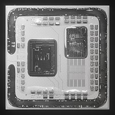
 Close-up of the I/O die
@Zen3@Vermeer@Ryzen_5_5600X@100-000000064_BG_2042SUS_9JF6228V00014_DSCx2.jpg)
@Zen3@Vermeer@Ryzen_5_5600X@100-000000064_BG_2042SUS_9JF6228V00014_DSCx4@IR.jpg)
@Zen3@Vermeer@Ryzen_5_5600X@100-000000064_BG_2042SUS_9JF6228V00014_DSCx3@IR.jpg)
In Zen 3, a single 32MB L3 cache pool is shared among all 8 cores in a chiplet, vs. Zen 2's two 16MB pools each shared among 4 cores in a core complex, of which there were two per chiplet. This new arrangement improves the cache hit rate as well as performance in situations that require cache data to be exchanged among cores, but increases cache latency from 39 cycles in Zen 2 to 46 clock cycles and halves per-core cache bandwidth, although both problems are partially mitigated by higher clock speeds. Total cache bandwidth on all 8 cores combined remains the same due to power consumption concerns. L2 cache capacity and latency remain the same at 512KB and 12 cycles. All cache read and write operations are done at 32 bytes per cycle.[13]
On April 20, 2022, AMD released the R7 5800X3D. It features, for the first time in a desktop PC product, 3D-stacked vertical L3 cache. Its extra 64MB comes via a TSMC N7 (7nm) "3D V Cache" die direct copper to copper hybrid bonded right on top of the 8-core Zen 3 CCD's usual 32MB, increasing the CPU's total L3 cache capacity to 96MB and bringing significant performance improvements for gaming in particular; now rivalling contemporary high-end consumer processors while being much more power efficient and running on older, cheaper motherboards using affordable DDR4 memory.[9] And despite now spanning multiple dies and being three times larger (96MB vs 32MB), the L3 cache's performance remains nearly identical; with X3D only adding around ≈+2ns via an additional three to four cycles of latency.[14] It would later be followed by the Ryzen 5 5600X3D and Ryzen 7 5700X3D for lower-end market segments, and succeeded by the Ryzen 7000X3D family of 3D V Cache equipped Zen 4 processors on the newer socket AM5 platform.
Improvements

Zen 3 has made the following improvements over Zen 2:[13][15]
- An increase of 19% in instructions per clock
- The base core chiplet has a single eight-core complex (versus two four-core complexes in Zen 2)
- A unified 32MB L3 cache pool equally available to all 8 cores in a chiplet, vs Zen 2's two 16MB pools each shared among 4 cores in a core complex.
- On mobile: A unified 16MB L3
- A unified 8-core CCX (from 2x 4-core CCX per CCD)
- Increased branch prediction bandwidth. L1 branch target buffer size increased to 1024 entries (vs 512 in Zen 2)
- New instructions
- VAES – 256-bit Vector AES instructions
- INVLPGB – Broadcast TLB flushing
- CET_SS – Control-flow Enforcement Technology / Shadow Stack
- Improved integer units
- 96 entry integer scheduler (up from 92)
- 192 entry physical register file (up from 180)
- 10 issue per cycle (up from 7)
- 256 entry reorder-buffer (up from 224)
- fewer cycles for DIV/IDIV ops (10...20 from 16...46)
- Improved floating point units
- Additional 64MB 3D vertically stacked dense library L3 cache (in -X3D models)
Feature tables
CPUs
This section is empty. You can help by adding to it. (March 2023) |
APUs
Products
Summarize
Perspective

On October 8, 2020, AMD announced four Zen 3-based desktop Ryzen processors, consisting of one Ryzen 5, one Ryzen 7, and two Ryzen 9 CPUs and featuring between 6 and 16 cores.[2]
Desktop CPUs
The Ryzen 5000 series desktop CPUs are codenamed Vermeer. The models in the second table are based on Cezanne APUs with the integrated GPU disabled. Meanwhile the Ryzen Threadripper Pro 5000 series were codenamed Chagall.
Common features of Ryzen 5000 desktop CPUs:
- Socket: AM4.
- All the CPUs support DDR4-3200 in dual-channel mode.
- All the CPUs support 24 PCIe 4.0 lanes. 4 of the lanes are reserved as link to the chipset.
- No integrated graphics.
- L1 cache: 64 KB per core (32 KB data + 32 KB instruction).
- L2 cache: 512 KB per core.
- Fabrication process: TSMC 7FF.
| Branding and model | Cores (threads) |
Thermal solution |
Clock rate (GHz) | L3 cache (total) |
TDP | Chiplets | Core config[i] |
Release date |
MSRP | ||
|---|---|---|---|---|---|---|---|---|---|---|---|
| Base | Boost | ||||||||||
| Ryzen 9 | 5950X | 16 (32) | — | 3.4 | 4.9 | 64 MB | 105 W | 2 × CCD 1 × I/OD |
2 × 8 | Nov 5, 2020 | US $799 |
| 5900XT | 3.3 | 4.8 | Jul 31, 2024 | US $349 | |||||||
| 5900X | 12 (24) | 3.7 | 2 × 6 | Nov 5, 2020 | US $549 | ||||||
| 5900 | 3.0 | 4.7 | 65 W | Jan 12, 2021 | OEM | ||||||
| PRO 5945 | Sep 2022[16] | ||||||||||
| Ryzen 7 | 5800X3D | 8 (16) | 3.4 | 4.5 | 96 MB | 105 W | 1 × CCD 1 × I/OD |
1 × 8 | Apr 20, 2022 | US $449 | |
| 5800XT | Wraith Prism | 3.8 | 4.8 | 32 MB | Jul 31, 2024 | US $249 | |||||
| 5800X | — | 4.7 | Nov 5, 2020 | US $449 | |||||||
| 5800 | 3.4 | 4.6 | 65 W | Jan 12, 2021 | OEM | ||||||
| 5700X3D | 3.0 | 4.1 | 96 MB | 105 W | Jan 31, 2024[17] | US $249 | |||||
| 5700X | 3.4 | 4.6 | 32 MB | 65 W | Apr 4, 2022 | US $299 | |||||
| PRO 5845 | Sep 2022 | OEM | |||||||||
| Ryzen 5 | 5600X3D | 6 (12) | 3.3 | 4.4 | 96 MB | 105 W | 1 × 6 | Jul 7, 2023 US Only[18] |
US $229[19] | ||
| 5600XT | Wraith Stealth | 3.7 | 4.7 | 32 MB | 65 W | Oct 31, 2024 | US $194[20] | ||||
| 5600X | 3.7 | 4.6 | Nov 5, 2020 | US $299 | |||||||
| 5600T | 3.5 | 4.5 | Oct 31, 2024 | US $186[20] | |||||||
| 5600 | 3.5 | 4.4 | Apr 4, 2022 | US $199 | |||||||
| PRO 5645 | — | 3.7 | 4.6 | Sep 2022 | OEM | ||||||
Common features of Ryzen 5000 (Cezanne) desktop CPUs:
- Socket: AM4.
- CPUs support DDR4-3200 in dual-channel mode.
- L1 cache: 64 KB (32 KB data + 32 KB instruction) per core.
- L2 cache: 512 KB per core.
- CPUs support 24 PCIe 3.0 lanes. 4 of the lanes are reserved as link to the chipset.
- No integrated graphics.
- Fabrication process: TSMC 7FF.
| Branding and model | Cores (threads) |
Thermal solution |
Clock rate (GHz) | L3 cache (total) |
TDP | Core config[i] |
Release date |
MSRP (USD) | ||
|---|---|---|---|---|---|---|---|---|---|---|
| Base | Boost | |||||||||
| Ryzen 7 | 5700[21] | 8 (16) | Wraith Stealth | 3.7 | 4.6 | 16 MB | 65 W | 1 × 8 | Apr 4, 2022 (OEM), Dec 21, 2023 (retail) |
$179 |
| Ryzen 5 | 5500 | 6 (12) | 3.6 | 4.2 | 1 × 6 | Apr 4, 2022 | $159 | |||
| Ryzen 3 | 5100[22][23][24] | 4 (8) | – | 3.8 | 8 MB | 1 × 4 | 2023 | OEM | ||
5100, 5500, and 5700 have no ECC support like non-Pro Ryzen 5000 Desktop APUs.
Common features of Ryzen 5000 workstation CPUs:
- Socket: sWRX8.
- All the CPUs support DDR4-3200 in octa-channel mode.
- L1 cache: 64 KB (32 KB data + 32 KB instruction) per core.
- L2 cache: 512 KB per core.
- All the CPUs support 128 PCIe 4.0 lanes. 8 of the lanes are reserved as link to the chipset.
- No integrated graphics.
- Fabrication process: TSMC 7FF.
| Branding and Model | Cores (threads) |
Clock rate (GHz) | L3 cache (total) |
TDP | Chiplets | Core config[i] |
Release date |
MSRP | ||
|---|---|---|---|---|---|---|---|---|---|---|
| Base | Boost | |||||||||
| Ryzen Threadripper PRO |
5995WX | 64 (128) | 2.7 | 4.5 | 256 MB | 280 W | 8 × CCD 1 × I/OD |
8 × 8 | Mar 8, 2022 (OEM) / ? (retail) |
OEM / US $6500 |
| 5975WX | 32 (64) | 3.6 | 128 MB | 4 × CCD 1 × I/OD |
4 × 8 | Mar 8, 2022 (OEM) / ? (retail) |
OEM / US $3300 | |||
| 5965WX | 24 (48) | 3.8 | 4 × 6 | Mar 8, 2022 (OEM) / ? (retail) |
OEM / US $2400 | |||||
| 5955WX | 16 (32) | 4.0 | 64 MB | 2 × CCD 1 × I/OD |
2 × 8 | Mar 8, 2022 | OEM | |||
| 5945WX | 12 (24) | 4.1 | 2 × 6 | |||||||
Desktop APUs
Cezanne
Common features of Ryzen 5000 desktop APUs:
- Socket: AM4.
- All the CPUs support DDR4-3200 in dual-channel mode.
- L1 cache: 64 KB (32 KB data + 32 KB instruction) per core.
- L2 cache: 512 KB per core.
- All the CPUs support 24 PCIe 3.0 lanes. 4 of the lanes are reserved as link to the chipset.
- Includes integrated GCN 5th generation GPU.
- Fabrication process: TSMC 7FF.
| Branding and model | CPU | GPU[a] | Thermal solution |
TDP | Release date |
MSRP | |||||||
|---|---|---|---|---|---|---|---|---|---|---|---|---|---|
| Cores (threads) |
Clock rate (GHz) | L3 cache (total) |
Core config[i] |
Clock (MHz) |
Config[ii] | Processing power[iii] (GFLOPS) | |||||||
| Base | Boost | ||||||||||||
| Ryzen 7 | 5705G | 8 (16) | 3.8 | 4.6 | 16 MB | 1 × 8 | 2000 | 512:32:8 8 CU |
2048 | — | 65 W | ||
| 5700G[b] | Wraith Stealth | Apr 13, 2021 (OEM), Aug 5, 2021 (retail) |
US $359 | ||||||||||
| 5705GE | 3.2 | — | 35 W | ||||||||||
| 5700GE[b] | Wraith Stealth | Apr 13, 2021 | OEM | ||||||||||
| Ryzen 5 | 5600GT | 6 (12) | 3.6 | 1 × 6 | 1900 | 448:28:8 7 CU |
1702.4 | 65 W | Jan 31, 2024[25] | US $140 | |||
| 5605G | 3.9 | 4.4 | — | ||||||||||
| 5600G[b] | Wraith Stealth | Apr 13, 2021 (OEM), Aug 5, 2021 (retail) |
US $259 | ||||||||||
| 5605GE | 3.4 | — | 35 W | ||||||||||
| 5600GE[b] | Wraith Stealth | Apr 13, 2021 | OEM | ||||||||||
| 5500GT | 3.6 | 65 W | Jan 31, 2024[25] | US $125 | |||||||||
| Ryzen 3 | 5305G | 4 (8) | 4.0 | 4.2 | 8 MB | 1 × 4 | 1700 | 384:24:8 6 CU |
1305.6 | — | |||
| 5300G[b] | OEM | Apr 13, 2021 | OEM | ||||||||||
| 5305GE | 3.6 | — | 35 W | ||||||||||
| 5300GE[b] | OEM | Apr 13, 2021 | OEM | ||||||||||
- Single precision performance is calculated from the base (or boost) core clock speed based on a FMA operation.
Mobile APUs
Cezanne
| Branding and Model | CPU | GPU | TDP | Release date | ||||||||
|---|---|---|---|---|---|---|---|---|---|---|---|---|
| Cores (Threads) |
Clock rate (GHz) | L3 cache (total) |
Core config[i] |
Model | Clock (GHz) |
Config[ii] | Processing power (GFLOPS)[iii] | |||||
| Base | Boost | |||||||||||
| Ryzen 9 | 5980HX[33] | 8 (16) | 3.3 | 4.8 | 16 MB | 1 × 8 | Radeon Graphics [a] |
2.1 | 512:32:8 8 CUs |
2150.4 | 35–54 W | Jan 12, 2021 |
| 5980HS[34] | 3.0 | 35 W | ||||||||||
| 5900HX[35] | 3.3 | 4.6 | 35–54 W | |||||||||
| 5900HS[36] | 3.0 | 35 W | ||||||||||
| Ryzen 7 | 5800H[37][38] | 3.2 | 4.4 | 2.0 | 2048 | 35–54 W | ||||||
| 5800HS[39] | 2.8 | 35 W | ||||||||||
| 5800U[note 1][40] | 1.9 | 10–25 W | ||||||||||
| Ryzen 5 | 5600H[41][42] | 6 (12) | 3.3 | 4.2 | 1 × 6 | 1.8 | 448:28:8 7 CUs |
1612.8 | 35–54 W | |||
| 5600HS[43] | 3.0 | 35 W | ||||||||||
| 5600U[note 1][44] | 2.3 | 10–25 W | ||||||||||
| 5560U[45] | 4.0 | 8 MB | 1.6 | 384:24:8 6 CUs |
1228.8 | |||||||
| Ryzen 3 | 5400U[note 1][46][47] | 4 (8) | 2.7 | 4.1 | 1 × 4 | |||||||
- Single precision performance is calculated from the base (or boost) core clock speed based on a FMA operation.
Barceló
| Branding and model | CPU | GPU | TDP | Release date | ||||||||
|---|---|---|---|---|---|---|---|---|---|---|---|---|
| Cores (Threads) |
Clock rate (GHz) | L3 cache (total) |
Core config[i] |
Model | Clock (GHz) |
Config[ii] | Processing power (GFLOPS)[iii] | |||||
| Base | Boost | |||||||||||
| Ryzen 7 | 5825U[note 1][note 2][51] | 8 (16) | 2.0 | 4.5 | 16 MB | 1 × 8 | Radeon Graphics[a] |
2.0 | 512:32:8 8 CUs |
2048 | 15 W | Jan 4, 2022 |
| Ryzen 5 | 5625U[note 1][note 2][52] | 6 (12) | 2.3 | 4.3 | 1 × 6 | 1.8 | 448:28:8 7 CUs |
1612.8 | ||||
| Ryzen 3 | 5125C[53] | 2 (4) | 3.0 | — | 8 MB | 1 × 2 | ? | 192:12:8 3 CU |
? | May 5, 2022 | ||
- Single precision performance is calculated from the base (or boost) core clock speed based on a FMA operation.
Barceló-R
Common features of Ryzen 7030 notebook APUs:
- Socket: FP6.
- All the CPUs support DDR4-3200 or LPDDR4-4266 in dual-channel mode.
- L1 cache: 64 KB (32 KB data + 32 KB instruction) per core.
- L2 cache: 512 KB per core.
- All the CPUs support 16 PCIe 3.0 lanes.
- Native USB 4 (40Gbps) Ports: 0
- Native USB 3.2 Gen 2 (10Gbps) Ports: 2
- Includes integrated GCN 5th generation GPU.
- Fabrication process: TSMC N7 FinFET.
| Branding and Model | CPU | GPU | TDP | Release date | |||||||
|---|---|---|---|---|---|---|---|---|---|---|---|
| Cores (threads) |
Clock rate (GHz) | L3 cache (total) |
Core config[a] |
Model | Clock (GHz) |
Processing power[b] (GFLOPS) | |||||
| Base | Boost | ||||||||||
| Ryzen 7 | (PRO) 7730U | 8 (16) | 2.0 | 4.5 | 16 MB | 1 × 8 | Vega 8 CU |
2.0 | 2048 | 15 W | January 4, 2023 [60] |
| Ryzen 5 | (PRO) 7530U | 6 (12) | 1 × 6 | Vega 7 CU |
1792 | ||||||
| 7430U | 2.3 | 4.3 | 1.8 | 1612.8 | Q4 2023 | ||||||
| Ryzen 3 | (PRO) 7330U | 4 (8) | 8 MB | 1 × 4 | Vega 6 CU |
1382.4 | January 4, 2023 [61] | ||||
- Single precision performance is calculated from the base (or boost) core clock speed based on a FMA operation.
Embedded CPUs
| Model | Release date |
Fab | CPU | Socket | PCIe support |
Memory support |
TDP | |||||
|---|---|---|---|---|---|---|---|---|---|---|---|---|
| Cores (threads) |
Clock rate (GHz) | Cache | ||||||||||
| Base | Boost | L1 | L2 | L3 | ||||||||
| V3C14[62][63] | September 27, 2022[64] | TSMC 7FF |
4 (8) | 2.3 | 3.8 | 32 KB inst. 32 KB data per core |
512 KB per core |
8 MB | FP7r2 | 20 (8+4+4+4) PCIe 4.0 |
DDR5-4800 dual-channel |
15 W |
| V3C44[62][63] | 3.5 | 3.8 | 45 W | |||||||||
| V3C16[62][63] | 6 (12) | 2.0 | 3.8 | 16 MB | 15 W | |||||||
| V3C18I[62][63] | 8 (16) | 1.9 | 3.8 | 15 W | ||||||||
| V3C48[62][63] | 3.3 | 3.8 | 45 W | |||||||||
Server CPUs
The Epyc server line of chips based on Zen 3 is named Milan and is the final generation of chips using the SP3 socket.[6] Epyc Milan was released on March 15, 2021.[65]
Common features:
- SP3 socket
- Zen 3 microarchitecture
- TSMC 7 nm process for the compute and cache dies, GloFo 14 nm process for the I/O die
- MCM with one I/O Die (IOD) and multiple Core Complex Dies (CCD) for compute, one core complex (CCX) per CCD chiplet
- Eight-channel DDR4-3200
- 128 PCIe 4.0 lanes per socket, 64 of which are used for Infinity Fabric in 2P platforms
- 7003X series models include 64 MiB L3 cache dies stacked on top of the compute dies (3D V-Cache)
- 7003P series models are restricted to uniprocessor operation (1P)
| Model | Cores (threads) |
Chiplets | Core config [i] |
Clock rate | Cache | Socket | Scaling | TDP default (range) |
Release price | |||
|---|---|---|---|---|---|---|---|---|---|---|---|---|
| Base (GHz) |
Boost (GHz) |
L2 (per core) |
L3 (per CCX) |
Total | ||||||||
| 7203(P) | 8 (16) | 2 + IOD | 2 × 4 | 2.8 | 3.4 | 512 KiB | 32 MiB | 68 MiB | SP3 | 2P (1P) | 120 W (120-150) | $348 ($338) |
| 72F3 | 8 + IOD | 8 × 1 | 3.7 | 4.1 | 260 MiB | 2P | 180 W (165-200) | $2468 | ||||
| 7303(P) | 16 (32) | 2 + IOD | 2 × 8 | 2.4 | 3.4 | 32 MiB | 72 MiB | 2P (1P) | 130 W (120-150) | $604 ($594) | ||
| 7313(P) | 4 + IOD | 4 × 4 | 3.0 | 3.7 | 136 MiB | 2P (1P) | 155 W (155-180) | $1083 ($913) | ||||
| 7343 | 3.2 | 3.9 | 2P | 190 W (165-200) | $1565 | |||||||
| 73F3 | 8 + IOD | 8 × 2 | 3.5 | 4.0 | 264 MiB | 240 W (225-240) | $3521 | |||||
| 7373X | 8* + IOD | 3.05 | 3.8 | 96 MiB | 776 MiB | 240 W (225-280) | $4185 | |||||
| 7413 | 24 (48) | 4 + IOD | 4 × 6 | 2.65 | 3.6 | 32 MiB | 140 MiB | 2P | 180 W (165-200) | $1825 | ||
| 7443(P) | 2.85 | 4.0 | 2P (1P) | 200 W (165-200) | $2010 ($1337) | |||||||
| 74F3 | 8 + IOD | 8 × 3 | 3.2 | 4.0 | 268 MiB | 2P | 240 W (225-240) | $2900 | ||||
| 7473X | 8* + IOD | 2.8 | 3.7 | 96 MiB | 780 MiB | 240 W (225-280) | $3900 | |||||
| 7453 | 28 (56) | 4 + IOD | 4 × 7 | 2.75 | 3.45 | 16 MiB | 78 MiB | 2P | 225 W (225-240) | $1570 | ||
| 7513 | 32 (64) | 4 × 8 | 2.6 | 3.65 | 32 MiB | 144 MiB | 2P | 200 W (165-200) | $2840 | |||
| 7543(P) | 8 + IOD | 8 × 4 | 2.8 | 3.7 | 272 MiB | 2P (1P) | 225 W (225-240) | $3761 ($2730) | ||||
| 75F3 | 2.95 | 4.0 | 2P | 280 W (225-280) | $4860 | |||||||
| 7573X | 8* + IOD | 2.8 | 3.6 | 96 MiB | 784 MiB | $5590 | ||||||
| 7R13[66] | 48 (96) | 6 + IOD | 6 × 8 | 2.65 | 3.7 | 32 MiB | 216 MiB | TBD | TBD | OEM/AWS | ||
| 7643(P) | 8 + IOD | 8 × 6 | 2.3 | 3.6 | 280 MiB | 2P (1P) | 225 W (225-240) | $4995 ($2722) | ||||
| 7663 | 56 (112) | 8 × 7 | 2.0 | 3.5 | 32 MiB | 284 MiB | 2P | 240 W (225-240) | $6366 | |||
| 7663P | 1P | 240 W (225-280) | $3139 | |||||||||
| 7713(P) | 64 (128) | 8 × 8 | 2.0 | 3.675 | 32 MiB | 288 MiB | 2P (1P) | 225 W (225-240) | $7060 ($5010) | |||
| 7763 | 2.45 | 3.4 | 2P | 280 W (225-280) | $7890 | |||||||
| 7773X | 8* + IOD | 2.2 | 3.5 | 96 MiB | 800 MiB | $8800 | ||||||
Zen 3+
Summarize
Perspective
| General information | |
|---|---|
| Launched | April 1, 2022 |
| Designed by | AMD |
| Common manufacturer | |
| CPUID code | Family 19h |
| Cache | |
| L1 cache | 64 KB (per core) |
| L2 cache | 512 KB (per core) |
| L3 cache | Up to 16 MB |
| Architecture and classification | |
| Technology node | TSMC N6 |
| Instruction set | AMD64 (x86-64) |
| Physical specifications | |
| Cores |
|
| Package |
|
| Products, models, variants | |
| Product code names |
|
| History | |
| Predecessor | Zen 3 |
| Successor | Zen 4 |
| Support status | |
| Supported | |
Zen 3+ is the codename for a refresh of the Zen 3 microarchitecture, which focuses on power efficiency improvements. It was released in April 2022 with the Ryzen 6000 series of mobile processors.
Features and improvements
Zen 3+ has 50 new or enhanced power management features over Zen 3, and also provides an adaptive power management framework, as well as new deep sleep states. Altogether, this brings improvements to efficiency both during idle, and when under load, with up to 30% performance-per-watt increase over Zen 3, as well as longer battery life.[67][68]
IPC is identical to that of Zen 3; the performance improvements of Ryzen 6000 over Ryzen 5000 mobile processors stem from it having a higher efficiency (hence more performance in power-constrained form factors like laptops), as well as the increased clock speeds from being built on the smaller TSMC N6 node.[69]
The Rembrandt implementation of Zen 3+ also has support for DDR5 and LPDDR5 memory.
Products
Rembrandt
On April 1, 2022, AMD released the Ryzen 6000 series of mobile APUs, codenamed Rembrandt. It introduces PCIe 4.0 and DDR5/LPDDR5 for the first time in an APU for the laptop and also introduced RDNA2 integrated graphics to the PC. It is built on TSMC's 6 nm node.[8]
Common features of Ryzen 6000 notebook APUs:
- Socket: FP7, FP7r2.
- All the CPUs support DDR5-4800 or LPDDR5-6400 in dual-channel mode.
- L1 cache: 64 KB (32 KB data + 32 KB instruction) per core.
- L2 cache: 512 KB per core.
- All the CPUs support 16 PCIe 4.0 lanes.
- Native USB 4 (40Gbps) Ports: 2
- Native USB 3.2 Gen 2 (10Gbps) Ports: 2
- Includes integrated RDNA 2 GPU.
- Fabrication process: TSMC N6 FinFET.
| Branding and model | CPU | GPU | TDP | Release date | ||||||||
|---|---|---|---|---|---|---|---|---|---|---|---|---|
| Cores (threads) |
Clock (GHz) | L3 cache (total) |
Core config[i] |
Model | Clock (GHz) |
Config[ii] | Processing power (GFLOPS)[iii] | |||||
| Base | Boost | |||||||||||
| Ryzen 9 | 6980HX | 8 (16) | 3.3 | 5.0 | 16 MB | 1 × 8 | 680M | 2.4 | 768:48:8 12 CUs |
3686.4 | 45 W | Jan 4, 2022 [70] |
| 6980HS | 35 W | |||||||||||
| 6900HX[a] | 4.9 | 45 W | ||||||||||
| 6900HS[a] | 35 W | |||||||||||
| Ryzen 7 | 6800H[a] | 3.2 | 4.7 | 2.2 | 3379.2 | 45 W | ||||||
| 6800HS[a] | 35 W | |||||||||||
| 6800U[a] | 2.7 | 15–28 W | ||||||||||
| Ryzen 5 | 6600H[a] | 6 (12) | 3.3 | 4.5 | 1 × 6 | 660M | 1.9 | 384:24:8 6 CUs |
1459.2 | 45 W | ||
| 6600HS[a] | 35 W | |||||||||||
| 6600U[a] | 2.9 | 15–28 W | ||||||||||
- Single precision performance is calculated from the base (or boost) core clock speed based on a FMA operation.
Rembrandt-R
Rembrandt-R is the codename for a refresh of Rembrandt codenamed processors, released as the Ryzen 7035 series of mobile APUs in January 2023.
Common features of Ryzen 7035 notebook APUs:
- Socket: FP7, FP7r2.
- All the CPUs support DDR5-4800 or LPDDR5-6400 in dual-channel mode.
- L1 cache: 64 KB (32 KB data + 32 KB instruction) per core.
- L2 cache: 512 KB per core.
- All the CPUs support 16 PCIe 4.0 lanes.
- Native USB 4 (40Gbps) Ports: 0
- Native USB 3.2 Gen 2 (10Gbps) Ports: 2
- Includes integrated RDNA 2 GPU.
- Fabrication process: TSMC N6 FinFET.
| Branding and model | CPU | GPU | TDP | Release date[79] | |||||||
|---|---|---|---|---|---|---|---|---|---|---|---|
| Cores (threads) |
Clock (GHz) | L3 cache (total) |
Core config[a] |
Model | Clock (GHz) |
Processing power[b] (GFLOPS) | |||||
| Base | Boost | ||||||||||
| Ryzen 7 | 7735HS | 8 (16) | 3.2 | 4.75 | 16 MB | 1 × 8 | 680M 12 CU |
2.2 | 3379.2 | 35–54 W | April 30, 2023 |
| 7735H | |||||||||||
| 7736U | 2.7 | 4.7 | 15–28 W | January 4, 2023 | |||||||
| 7735U | 4.75 | 15–30 W | |||||||||
| 7435HS | 3.1 | 4.5 | — | 35–54 W | 2024[80] | ||||||
| 7435H | |||||||||||
| Ryzen 5 | 7535HS | 6 (12) | 3.3 | 4.55 | 1 × 6 | 660M 6 CU |
1.9 | 1459.2 | April 30, 2023 | ||
| 7535H | |||||||||||
| 7535U | 2.9 | 15–30 W | January 4, 2023 | ||||||||
| 7235HS | 4 (8) | 3.2 | 4.2 | 8 MB | 1 × 4 | — | 35–53 W | 2024[81] | |||
| 7235H | |||||||||||
| Ryzen 3 | 7335U | 3.0 | 4.3 | 660M 4 CU |
1.8 | 921.6 | 15–30 W | January 4, 2023 | |||
- Single precision performance is calculated from the base (or boost) core clock speed based on a FMA operation.
References
Wikiwand - on your browser
Seamless Wikipedia browsing. On steroids.
Welcome to Wikiwand👋
Wikipedia – from the future